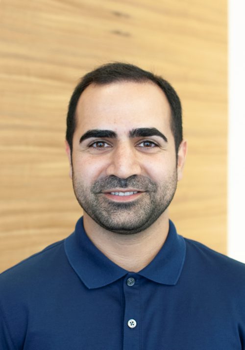
Skip to content

News & Events

Scientists engineer a functional optical lens out of 2D materials

In a paper published Oct. 8 in the journal Nano Letters, a team from the University of Washington and the National Tsing Hua University in Taiwan announced that it has constructed functional metalenses that are one-tenth to one-half the thickness of the wavelengths of light that they focus. Their metalenses, which were constructed out of layered 2D materials, were as thin as 190 nanometers — less than 1/100,000ths of an inch thick.

UW Electrical & Computer Engineering department hiring tenure-track faculty

The Department of Electrical & Computer Engineering (ECE) at the University of Washington, Seattle invites applications for multiple full-time tenure-track positions with a nine-month service period annually, from exceptional candidates with strong record of collaboration and creativity. Hiring will be made primarily at the tenure-track assistant professor level with an anticipated start date of September 16, 2019. More information about the department, including background on our recent name change to ECE can be found at www.ece.uw.edu.

Shreyas Shah awarded Mistletoe Research Fellowship

Dr. Shreyas Shah, a postdoc working with Karl Böhringer and Arka Majumdar on an integrated photonics project, has been awarded an Unfettered Research Grant award to the tune of $10,000 by the Mistletoe Research Foundation. The Mistletoe Research Foundation, founded in 2017, builds bridges between the academic, entrepreneurial, and civil communities to create a more human-centered and sustainable future through technology.

AFM Workshop for Scanning Microwave Impedance, May 1, 10:00 – 11:30 am, MolES 215

PrimeNano will give a talk on the method May 1st from 10:00 am – 11:30 am in MolES 215.  They will then provide demos on the technique using our AFM Dimension Icon that afternoon and the next day.

Speaker Bio: Oskar Amster, M.S. (Sr. Dir. Marketing of PrimeNano, Inc)

Mr. Amster has a background in Physics and Materials engineering with a focus on microelectronics processing. He has 20 years experience working with analytical instruments and metrology tools. His background is in applications development, strategic marketing, and product development. He has extensive experience working in Atomic Force Microscopy, Stylus Profilers, and Optical Profiler instruments. Prior to joining PrimeNano, Inc, Oskar was at KLA-Tencor and also held positions at several start-ups as well as mature instrument companies. He holds an MS in Materials Engineering and BS in Physics from Cal Poly San Luis Obispo.

ScanWave sMIM Presentation Abstract

Yoshikazu Hirai, University of Kyoto – Body-on-a-Chip: an application of three-dimensional microstructuring techniques: April 13, 10:30 am, NanoES 291

Body-on-a-Chip: an application of three-dimensional microstructuring techniques

Yoshikazu HIRAI
Department of Micro Engineering, Kyoto University, JAPAN
E-mail: hirai@me.kyoto-u.ac.jp
http://www.nms.me.kyoto-u.ac.jp/en/member/hirai/

NanoES 291

Abstract
This presentation introduces three-dimensional (3-D) microstructuring methods based on optical lithography and addresses one of their application for developing “Body-on-a-Chip.” In vitro cell-based assay with human cells is getting attention since the accuracy of preclinical predictions of drug responses should be improved to reducing costly failures in clinical trials. In order to generate reliable predictions, we have developed a micro-engineered biomimetic systems “Body-on-a-Chip,” to investigate the effects of drugs/metabolites on multi organs by assembling a closed-loop medium circulation system on one microfluidic device. For 3-D polymeric sensor/actuator device fabrication, an advanced 3-D lithography with the process optimization was applied to improve device performances. Our Body-on-a-Chip was successfully applied to evaluate the effect of an anti-cancer drug (doxorubicin) on cell survival of human heart and liver cells.

Biography
Yoshikazu Hirai received the B.S. and M.S. degrees from Ritsumeikan University, Japan, in 2002 and 2004, respectively, and the Ph.D. degree from Kyoto University, Japan, in 2007, all in mechanical engineering. He was a Post-doctoral Researcher with the Graduate School of Engineering, Kyoto University. In 2009, he joined the Advanced Biomedical Engineering Research Unit, Kyoto University. Since 2013, he has been an Assistant Professor with the Department of Micro Engineering, Kyoto University. Dr. Hirai was a recipient of the Outstanding Reviewer Award in 2016 (Journal of Micromechanics and Microengineering, IoP) and the Institute of Electrical Engineers of Japan (IEEJ) Distinguished Paper Award in 2017. His current research interests include (1) Fabrication and packaging technologies for MEMS, (2) Optical lithography for 3D microstructuring, (3) Atomic sensor device (e.g., CSAC: Chip Scale Atomic Clock, CSAM: Chip Scale Atomic Magnetometer), and (4) Microfluidic system/device for biomedical applications.