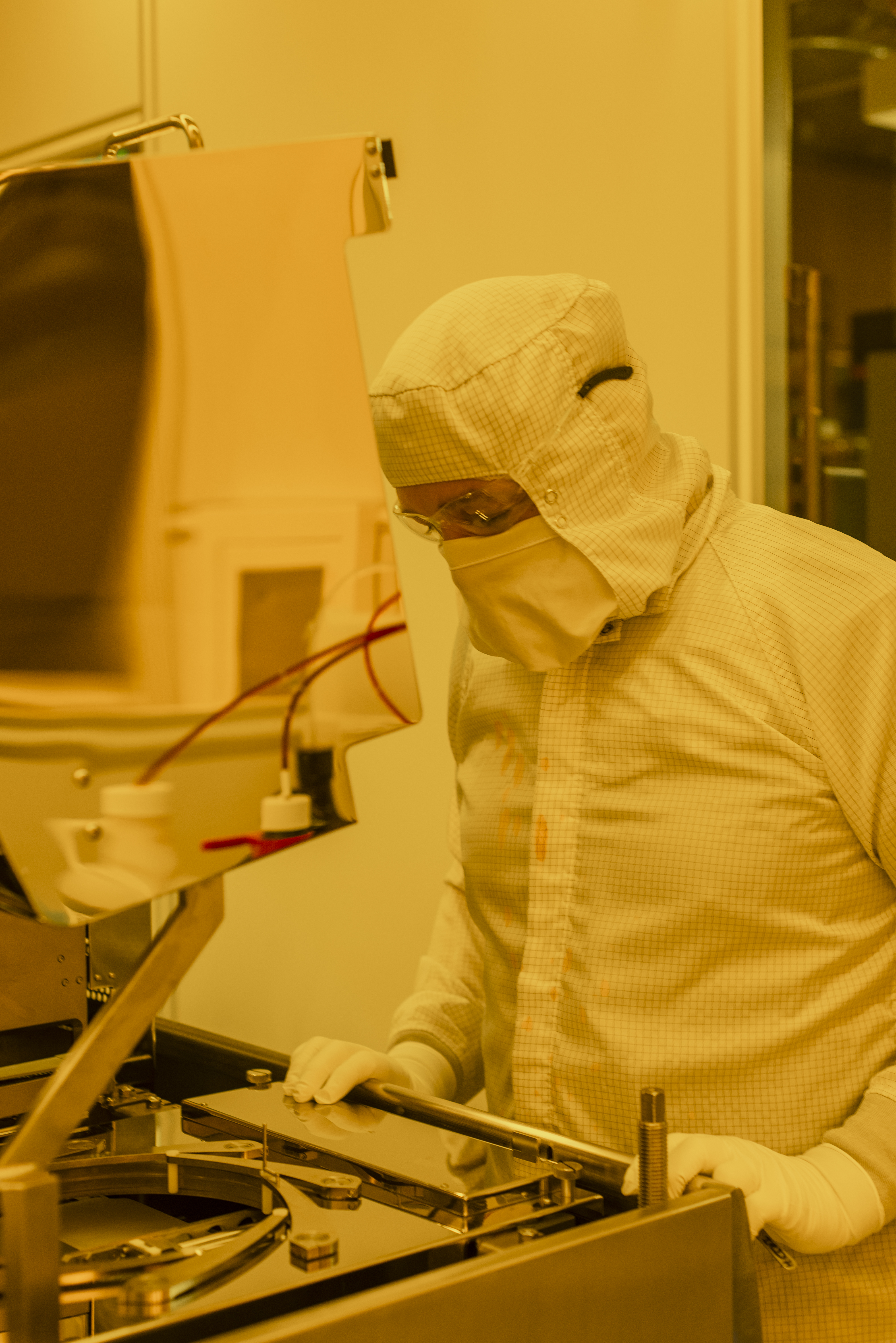
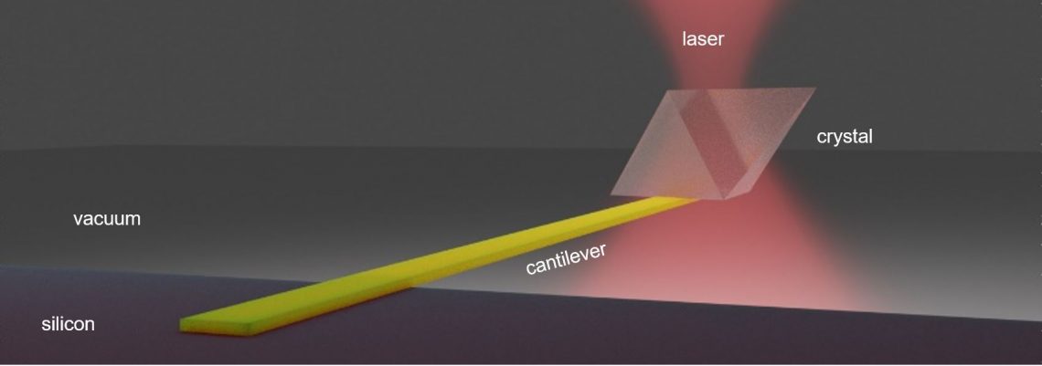
Skip to content

News & Events

Defects Wanted; Apply Here – Q&A with physicist Kai-Mei Fu

NanoES faculty member and professor of electrical engineering and physics recently sat down with APS Physics. Kai-Mei studies the properties of atomic defects in materials with the goal of using these normally unwanted flaws to create quantum technologies for secure communication. She is also the co-chair of QuantumX, a University of Washington initiative seeking to facilitate and support activities that will accelerate quantum discoveries and technologies

First-ever visualizations of electrical gating effects on electronic structure could lead to longer-lasting devices

UW physicists David Cobden and Xiaodong Xu, in collaboration with colleagues at the University of Warwick, developed a technique to measure the energy and momentum of electrons in operating microelectronic devices made of atomically thin — so-called 2D — materials. Their findings, published last week in the journal Nature could lead to new, finely tuned, high-performance electronic devices.

Researchers take a bottom-up approach to synthesizing microscopic diamonds for bioimaging, quantum computing

NanoES faculty member Peter Pauzauskie and his team discovered that they can use extremely high pressure and temperature to introduce other elements into nanodiamonds, making them potentially useful in cell and tissue imaging, as well as quantum communications and quantum sensing. This work was done in collaboration with the U.S. Naval Research Laboratory and the Pacific Northwest National Laboratory and published in Science Advances on May 3.