By Wayne Gillam | UW ECE News

It might not be commonly known, but artificial intelligence and machine learning applications are commonplace today, performing a multitude of tasks for us behind the scenes. For example, AI and machine learning helps to interpret voice commands given to our phones and devices such as Alexa, recommends movies and music we might enjoy through services such as Netflix and Spotify, and is even driving autonomous vehicles. In the near future, the reach of AI and machine learning applications is expected to extend even further, to more complex tasks such as supporting space missions and defense operations, and developing new drugs to treat disease.
But the growing sophistication of AI and machine learning applications, as well as their implementation at such a large scale, demands a need for computing power which roughly doubles every three to four months. That’s much faster than Moore’s law (the observation that the number of transistors in a dense, integrated circuit doubles about every two years). Conventional computing paradigms and hardware platforms are having trouble keeping up. Also, cloud computing data centers used by AI and machine learning applications around the world currently gobble up an estimated 200-terawatt hours per year. That’s more than a small country. It’s easy to see that this energy consumption will come hand-in-hand with serious environmental consequences.
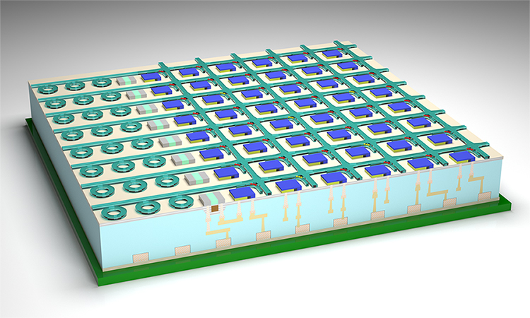
To help address these challenges, UW ECE faculty members Sajjad Moazeni and Mo Li are leading a multi-institutional research team that recently received a four-year grant from the National Science Foundation to develop a new type of computer chip that uses laser light for AI and machine learning computation. This chip, called a “hybrid co-processing unit,” or HCU, stands to greatly accelerate the computing speed and efficiency of AI and machine learning applications, while at the same time reducing energy consumption. The computational power of the HCU will be over ten times greater than today’s most advanced silicon-based microprocessors of comparable size.
“There is a need to shift the computing paradigm to something new,” said Moazeni, who is lead principal investigator of the project. “One of the most important and distinctive novelties in the work we are doing is that what we are proposing can very tightly get integrated with existing silicon-based microprocessors in today’s data centers. That is something very unique.”
A new, scalable optical computing paradigm
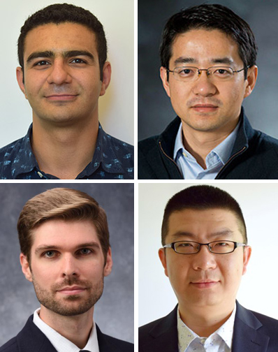
The research team developing the HCU, top row, left to right: UW ECE Assistant Professor Sajjad Moazeni, UW ECE Professor Mo Li. Bottom row, left to right: Nathan Youngblood, an assistant professor of electrical and computer engineering at the University of Pittsburgh, Lei Jiang, an assistant professor of intelligent systems engineering at Indiana University Bloomington

The HCU combines traditional electronics with photonics, using light generated by lasers instead of electricity for data processing. The device does this by way of an optical computing core that includes phase-change material (a substance similar to what is in CD-ROMs and DVDs) to record information. This computing core can realize an optical neural network on the chip to accelerate computational speed in an ultracompact footprint, storing data on-chip using the phase-change material at essentially zero-power.
“The HCU is a single-chip solution that can be integrated with today’s silicon-based microprocessors,” Moazeni said. “We call it ‘hybrid’ because we are co-optimizing the benefits of electronics, photonics and phase-change materials, all within one system.”
The project builds on research by Moazeni, who is an expert in large-scale integrated photonics and microelectronics, as well as Li, who has been developing optical computing systems using phase-change materials at UW ECE. According to Moazeni and Li, this is the first time photonics and electronics have been so tightly integrated together in a single chip for the purpose of accelerating AI and machine learning computations.
“Optical computing is best for data movement and linear computation, while traditional electronics are really good at digital computation and also implementing nonlinear algorithms, which optical computing cannot easily do,” Li said. “Our strategy combines the best of the two.”
Other members of the research team are Nathan Youngblood, an assistant professor of electrical and computer engineering at the University of Pittsburgh, and Lei Jiang, an assistant professor of intelligent systems engineering at Indiana University Bloomington. Youngblood will work on designing electrically programmable, high density optical memory arrays for ultrafast optical computation, and Jiang will be focusing on optimizing the device for accelerating emerging AI and machine learning applications.
What’s next?
The research team is working toward combining the phase-change material with microelectronics circuitry at the Washington Nanofabrication Facility. This will be achieved through integrating the phase-change material with an advanced silicon photonic process fabricated at a commercial foundry. The method allows thousands of photonic elements and millions of transistors to be fabricated together in a cost-effective and scalable manner. The team will also be building computer models to simulate every aspect of the device.
“We’ll start by modeling and putting together the full end-to-end model of the HCU, model the phase-change material, model the photonics and construct a new, unique framework on which we can simulate all of them together,” Moazeni said.
By the end of the NSF grant in 2025, the research team expects to have a working, physical prototype. Then, the group will be poised to manufacture the device in larger quantities and at a scale capable of moving into the marketplace.
What does that mean for the rest of us? Eventually, the work promises to translate into quicker response times and improved performance for any computer application that involves AI or machine learning (such as our phones, Alexa, Netflix and Spotify). It also will help make possible a significant reduction in energy consumption, making technology driven by AI and machine learning more environmentally friendly.
“This is the first time that we’ll be bringing a non-traditional computing chip into the real world for practical applications, and I’m really excited about that,” Moazeni said. “It’s a realization of Moore’s law, which stated that eventually new materials would need to be brought into chip development in order to increase computing capacity and speed.”
“Our technology will improve speed, performance and power consumption,” Li added. “And perhaps most importantly, it will help to put AI computing on a sustainable energy path.”
For more information about research described in this article, contact Sajjad Moazeni or Mo Li.